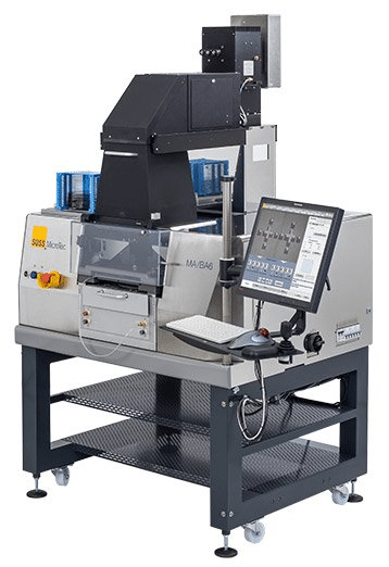
Fabrication Micro- and Nanopatterning

Micro- and nanolithography is a key technology in manufacturing of integrated circuits and microchips that allows for creating patterns with a feature size from nanometer up to millimeter scale. Lithography techniques can be divided into two types: masked lithography and maskless lithography. Masked lithography such as photolithography and nanoimprint lithography makes use of masks to transfer patterns over a large area simultaneously making the process cost-effective. Maskless lithography such as electron beam lithography and laser writing enable arbitrary patterns with high-resolution and a minimum feature size as small as a few nanometers.