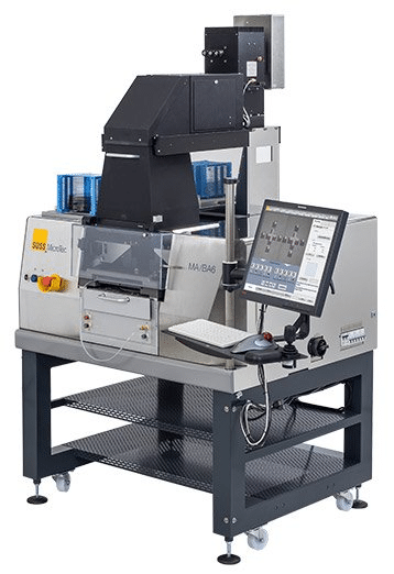
Top side UV-lithography, Bottom side UV-lithography, Micro and nanoimprint lithography (SMILE), UV-bonding
Details
Optical and nano imprint lithography, wafer adhesive bonding
Suss MA6 is an mask aligner system capable to perform several different type of task. Equivalent tools is found in VTT/Oulu and in Tampere University. The tool installed at Tampere contains options to:
- Top side UV-lithography
- Bottom side UV-lithography
- Micro and nanoimprint lithography (SMILE)
- UV-bonding
Lithography
Typical lithography run includes coating substrate with UV-polymer or photo-resist and pre-baking it prior loading to aligner. UV-light is used as a tool to define areas that are either soluble or insoluble to developer. Top side lithography refers to case where the substrate is viewed through photomask to allow alignment of patterns pre-existing on a front side of the substrate to patterns on mask.
Our tool is also equipped with bottom side lithography option allowing one to align patterns pre-existing on the bottom side of the substrate to patterns generated on the top side. This is achieved by using bottom side microscope below the substrate to image mask position prior the substrate is loaded (to block view). Once the position of the mask patterns is known the substrate is loaded and bottom side of the substrate is viewed with the bottom side microscope. Pre-stored mask image is overlayed with live bottom image allowing their simultaneous alignment. Once alignment is completed wafer can be exposed through the mask and the pattern is generated on the topside. This generated pattern is in precise alignment with the bottom side patterns.
Resolution of the patterns is largely dictated by gap between photo-resist and mask surface. System has different contact modes as listed below that influence on the gap depth. Obviously, the modes where the mask is forded to contact with the substrate allow higher resolution but at the same time can contaminate the mask and the substrate. Vacuum contact mode is so strong that it can bend the mask and is not generally advised to be used.

Imprint lithography
Imprint lithography utilizes large thin UV-transparent glass or PET foils to act as a working stamp. Separate tool is used to replicate on top of this foil nano or micropattern from template/master wafer. User loads foil into the system and a substrate with UV-curable polymer. Aligner brings patterned stamp surface into contact with UV-polymer and applies force to evacuate gas trapped between two surfaces. Once contact is achieved UV-lamp of the tool cures UV-polymer and tool rips stamp from cured polymer.
UV-bonding
Tool is used to bring two substrates in contact (and align them). If interface between substrates is covered with UV-curable polymer it is possible to cure expose through top surbstrate and cure UV-polymer.
Nominal Specifications
Substrate max thickness 1.5 mm in vacuum contact and 7 mm in other modes
Illumination uniformity +/- 2.5%
Light source: UV-LED. 3 individually adjustable lines
- 365 nm (i-line)
- 405 nm (h-line)
- 435 nm (g-line)
Two exposure optics settings:
- For large gap between mask and substrate
- For large resolution
Alignment accuracy:
- Top side < 0.5 µm (0.25 µm with auto-align software)
- Bottom side < 1 µm
- Imprint < 2 µm
Available tools
Wafer chucks:
6″ wafer chuck, lithography, vacuum, hard, soft and proximity contact.
Small sample holder, 5×5 mm^2 to 4″ area, other contact modes than vacuum. Double side lithography.
For 100mm wafers, with all contact modes. Double side lithography.
Mask holder:
For small samples: aperture 30.8 x 30.8 mm^2, mask 2″ or 4″
For 5″ or 6″ mask with 100 mm by 100 mm aperture
For 4″ mask and 3″ aperture
Stamp holder for thinner than 3mm stamps, aperture 150 mm
Objectives:
Offset objective, 16.7 mm min distance between alignment marks, 7.2X magnification, 17 mm working distance.
Standard objectives, 5x magnification, 29 mm min distance between alignment marks, 20 mm working distance.
Bottom side microscope, 15 mm min distance between alignment marks.

Movement ranges for top stage in topside (MA) lithography and in bottom side (BA) lithography. Movement limits for bottom side microscope.
Send an enquiry
"*" indicates required fields
Select recipient for your enquiry:

