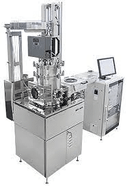
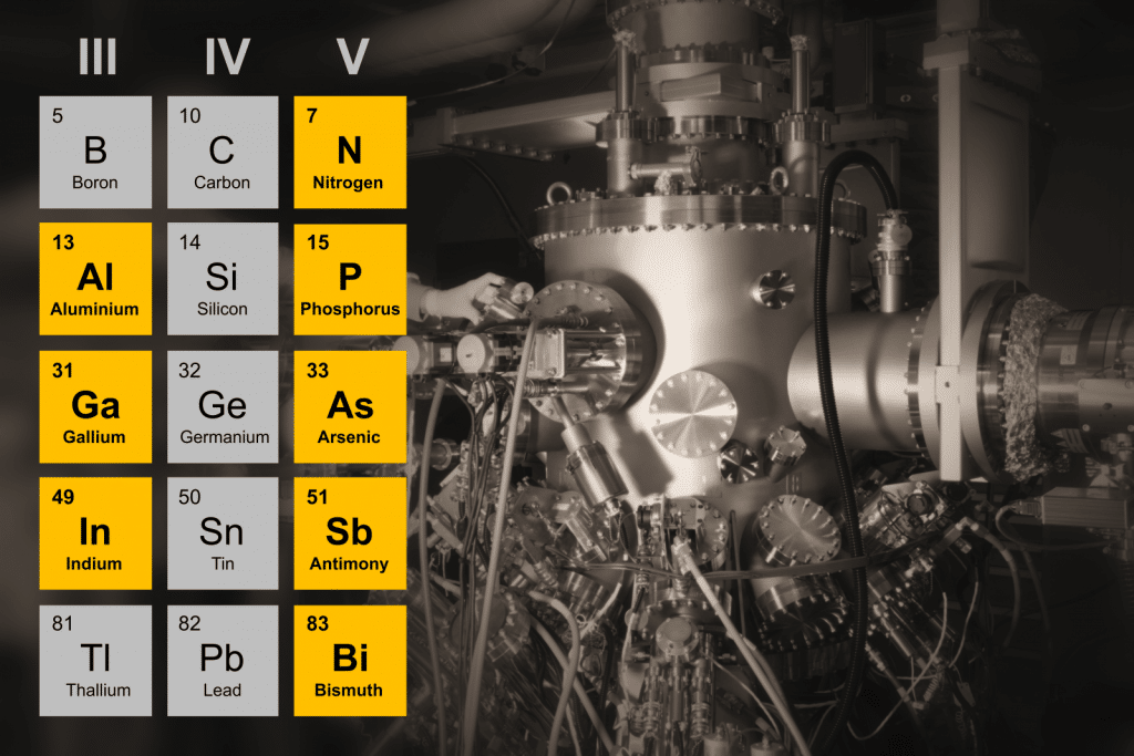
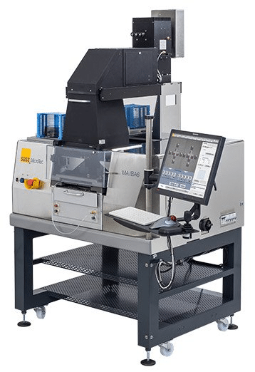
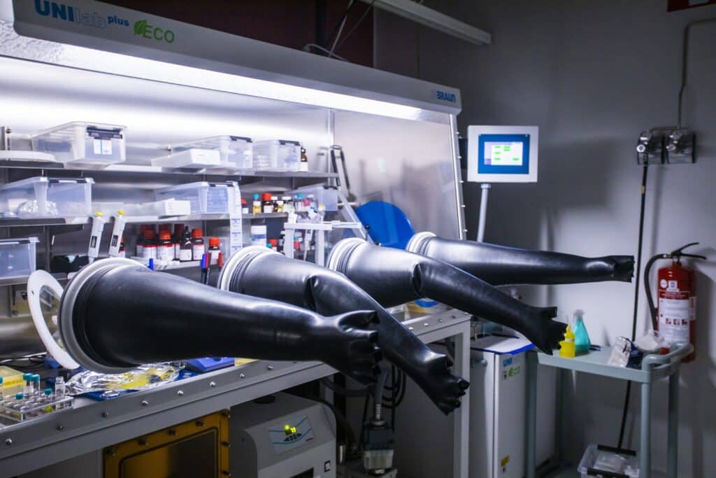
Fabrication Micro- and Nanopatterning
Our capabilities cover a wide range of materials including carbon-based materials, semiconductors, photovoltaic materials, coatings, thin-films, and glasses. We also have a wide range of fabrication methods including epitaxy, lithography, atomic layer deposition, and 3D printing optics.