
IBS NAVIGATOR 700 (Cutting Edge Coatings GmbH, 2016) is an optical coater designed for automatic coating of planar glass substrates. The system utilizes broadband optical monitoring (BBM) through monitor fused silica windows or layers can be deposited using time control.
Details
Location:
Tampere University (TAU), University of Eastern Finland (UEF), Joensuu, Tampere
Contact persons:
Jukka Viheriälä (Tampere), Petri Karvinen (Joensuu)
Info:
IBS NAVIGATOR 700 (Cutting Edge Coatings GmbH, 2016) is an optical coater designed for automatic coating of planar glass substrates. The system utilizes broadband optical monitoring (BBM) through monitor fused silica windows or layers can be deposited using time control. Main deposition method is reactive sputtering of metallic targets in O2 atmosphere (~4E-4mbar). The system is also equipped with a secondary ion source for ion assisted deposition and sample cleaning/preparation.
Typical coating run includes sample loading and preparations (~15 min), pumping the system to base pressure (~15 min), warming up the ion sources (~30 min), the actual deposition (~coating thickness per 0.15 nm/s), cooling period ( ~10 min) and sample evacuation plus clean-up (~15 min). So roughly 1.5 hours plus the deposition time. BBM can reliably monitor layer thicknesses above 30 nm, but this is also material dependent (refractive index contrast to fused silica). Automatic coating runs require a recipe file .dsg, which is a file format by Laser Zentrum Hannover “Spectrum” software. With automatic deposition user can deposit only two materials at a coating run, one high refractive index material (TiO2/ Ta2O5) and one low refractive index material (SiO2/ Al2O3). More materials require active operator adjustments during the coating run.
Spesifications
The system is mainly reserved for transparent materials, as the possibility of cross-contamination and increased losses in coatings are supposed to be kept in minimum. Some exotic tests are possible with careful pre-considerations, like nitride depositions or assist source cleaning, but require contacting responsible person beforehand and getting their approval for the wanted process.
Coating Materials: SiO2, TiO2, Al2O3, Ta2O5, (SiNx, AlNx)
Sputtering uses Ar/O2 (8:5 sccm) ion beam, backed with ~80 sccm O2 process gas flow.
Assist source gases: H2, O2, N2, Ar
Typical substrates: Fused silica, Quartz, BK7, Si, GaAs
Typical coatings: Laser mirrors on lenses, Anti-reflection (AR) coatings, High-reflection (HR) mirrors, Laser diode coatings (AR/HR), Passband/Stopband filters, Polarizing coatings.
Training Requirements
For a user to get training for the IBS, they must have:
- Frequent need (a series of filters, established need for regular coating runs, a specific thesis work related to sputtering, etc.)
- Established know-how of optical coatings (be familiar with the physical vapor deposition methods in general, understand the basic principles of designing optical filters)
- The research group/company doesn’t have several available personnel already trained for the system (For the system and resources it is better to have few regular users than many doing deposition now and then)
If these requirements aren’t fulfilled, it is possible to get few coatings done by the responsible operator.
Not allowed processes
Just to name a few unallowed processes and reasons why they are not usable. Any non-standard process needs approval from the responsible person for the same reasons than listed below.
- Gold deposition/Other pure metals: Contamination risk of the existing processes, blocking the optical monitoring.
- Zinc based processes (ZnO, other zinc materials): Zinc has high vapor pressure and it diffuses everywhere, causing contamination of the entire system.
- Other high vapor pressure/volatile materials: Contamination.
- Extended etching times (~>10 min): Cross-contamination and contamination of target materials.
Joensuu
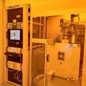
Kurt J. Lesker LAB 18
- 45 cm x 45 cm x 50 cm chamber size (D-shaped)
- 6″ x 6″ Max. sample size
- Electron beam source with 4 pockets, 5 kW
- 4″ DC sputtering source, 2 kW
- Substrate heating to 550 °C
- Ar and/or O2 atmosphere
- Material include: Al, Al2O3, Cr, Cu, Ge, ITO, SiO2, TiN, TiO, TiO2, TiW
Moorfield MiniLab 026
- 31 cm x 30 cm x 35 cm (round)
- 6″ x 6″ Max. sample size
- Dual thermal source 1000 W
- 3″ RF sputtering source 300 W
- O2 atmosphere
- Materials include: Ag, Al, Au, Cr, Cu

Send an enquiry
"*" indicates required fields
Select recipient for your enquiry: