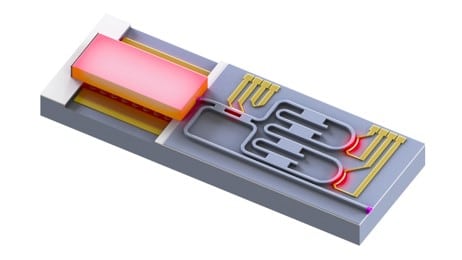
Most demanding flip-integration with sub-micron accuracy is needed for e.g. waveguide-waveguide coupling
Details
Location:
VTT, Espoo, Oulu, Tampere
Info:
FinnLight consortium has the tools and experience for the most demanding flip-chip bonding tasks. For example, semiconductor optical amplifier (SOA) waveguide chips can be bonded up-side-down on silicon-on-insulator (SOI) waveguide chips to realize external cavity lasers. Because of the small mode-field diameters in the waveguides (<3 µm) the optical axes of the waveguides have to be aligned with sub-micron precision. Vertical alignment is typically done passively with mechanical standoff structures, while the horizontal alignment is achieved with high-resolution cameras that align the chips with respect to each other before the bonding.
High-precision flip-chip bonding at VTT in Espoo (Contact person Jae-Wung Lee)
New Finetech FEMTO2 flip-chip bonder was installed into Micronova clean room in 2023 and it will be used for the most demanding flip-chip bonding tasks, such as III-V compound semiconductor chip bonding on SOI waveguide chips and wafers. Nominal placement accuracy of the tool is 0.3 µm (3 sigma). This tool supports fully automated chip-to-wafer bonding, as well as chip-to-chip bonding.
- Contact person: Jae-Wung Lee
- https://finetech.de/products/fineplacer-femto-2/
High-precision flip-chip bonding at VTT in Oulu (Contact person Jaska Paaso)
Finetech FINEPLACER® sigma flip-chip bonder can be used for the most demanding flip-chip bonding tasks. This tool enables manual and semi-automated chip-to-chip bonding with a nominal placement accuracy of 0.5 µm.
- Contact person: Jaska Paaso
- https://finetech.de/products/fineplacer-sigma/
Ultra-precise die and flip-chip bonder
System Description
SET ACCµRA Plus (SET, 2024) is very versatile and accurate to different type of scenarios to bond or stack chips on different type of chip carriers, interposers and substrates. Bonding is possible with solder, metal-metal interface, glue and sintering process.
Some highlights:
- 0.5 µm 3 sigma chip bonding accuracy
- Thermocompression bonding up to 450degC and ultrasonic bonding
- Sintering processes to up to 100 bar limited by 1000N
- Tool is configured to C2C processing but upgradable to C2W up to 200mm diam. wafers
- Time-pressure fluid dispenser and dip-tray to apply adhesives (and UV-curing lamps for UV-adhesives)
- Automatic die-ejector system for up to 200 mm wafers and chip-flip module. Die presentation with 2” and 4” chip trays.
- Chip sizes from ~0.2×0.2 mm2 range to 50×50 mm2 range
- Automatic mode for up to ~120 chips per hour range
-
Cognex-based optical pattern recognition for chip and substrate alignment.
Functionalities
System contains two robots. A highly precise bonding robot handles the chip alignment and bonding, and less precise transfer robot handles feeding the parts for the bonding robot.

Contact person: Jukka Viheriälä
Send an enquiry
"*" indicates required fields
Select recipient for your enquiry: