
We provide thin-film deposition using ALD, PECVD, Langmuir-Blodgett molecular layer deposition, and physical vapour deposition methods such as electron beam/thermal evaporation and magnetron sputtering. This ensures precise control of thickness and uniformity.
Details
Location:
Tampere University (TAU), University of Eastern Finland (UEF), Joensuu, Tampere
Contact persons:
Aleksander Vlasov (Tampere), Pertti Pääkkönen (Joensuu)
Info:
Many photonics applications require nanoscale features, and their performance and reliability depend on precise fabrication techniques. Thin-film deposition is a critical step in this process, as it directly affects the optical properties, layer uniformity, and device functionality of the final product. Deposition methods can be categorised as follows:
- Physical deposition, where the target material is transferred to the substrate by physical means (e.g., sputtering, thermal, and electron-beam (E-beam) evaporation).
- Chemical deposition, where the chemistry of precursor gases is exploited to achieve the desired coatings (e.g. chemical vapor deposition (CVD), plasma enhanced CVD (PCVD), and atomic layer deposition (ALD)).
Atomic layer deposition (ALD)
ALD offers a key advantage over CVD, PVD, and sol-gel: it produces highly conformal films, even on complex 3D structures like vertical nanowires and porous surfaces. It also enables selective deposition on chemically pre-patterned areas.
However, drawbacks include slow growth rates of ~0.1 nm per cycle (typically 10–50 nm/h) and the requirement for substrates to be chemically reactive and resistant to process conditions such as heating. Most ALD processes are carried out at temperatures between 100 and 400 °C.
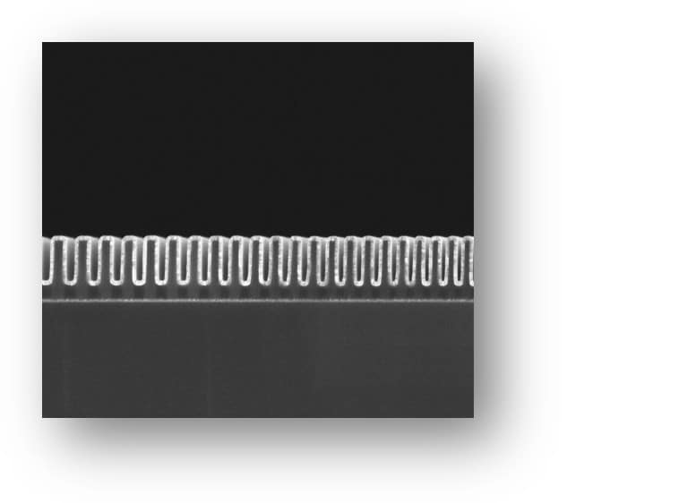
An example of a conformally deposited sample.
Beneq ALD TFS 200
UEF’s ALD system supports both thermal and plasma-enhanced ALD, offering flexibility in precursor selection and process conditions.
Deposited materials and their precursors.
| Material | Precursors |
| Al2O3 | TMA + H2O |
| TiO2 | TiCl4 + O2 |
| SiO2 | BEMAS + O3 |
Characteristics
- Interchangeable thermal and plasma-assisted chambers for
- Increased precursor selection range
- Controlled deposition rate
- Controlled uniformity and conformality.
- Four liquid precursor lines and two hot sources (300 °C and 500 °C) for
- Cross-contamination control – separate lines
- Improved efficiency
- Simultaneous processing
- Control of individual precursor lines.
- Ozone source
- Essential for high-quality oxides.
- Sample and process information
- substrate size: up to 8-inch
- Reactor temperature: 300 oC max.
Picosun Sunale ALD R-200
TAU’s system supports both thermal and plasma-enhanced ALD, offering flexibility in precursor selection and process conditions.
Deposited materials and their precursors:
| Material | Precursors |
| AlOx | TMA + H2O |
| TiOx | TDMAT + H2O |
| FeOx | FCl + H2O |
Characteristics
- Supports both thermal and plasma-enhanced ALD modes for
- Broad precursor compatibility
- Controlled deposition rate
- Controlled uniformity and conformality.
- Up to 6 sources with 4 separate inlets for
- Cross-contamination control – fully separated inlets
- Improved efficiency
- Simultaneous processing
- Control of individual precursor lines.
- Ozone source
- Essential for high-quality oxides.
- Sample and process information
- substrate size: up to 8-inch, height max. 0.5”
- Reactor temperature: thermal up to 500 °C, plasma ~450 °
Plasma Enhanced Chemical Vapor Deposition (PCVD)
TAU has two Plasmalab 80+ Plasma Enhanced Chemical Vapor Deposition systems (PECVDs) (Oxford Plasma Technology, 2000), which are used for thin film growth and plasma treatments. Normal process temperature is 300 °C, with an operable range from room temperature to 400 °C. The systems are dedicated to SiNx and SiO2 growth. Both systems can deposit both materials and materials can also be used in combination if necessary.
Specifications:
- Process gases: N2, N2:SiH4 2 %, N2O, NH3, (CHF4/O2 as cleaning gas)
- Typical substrates: Fused silica, Quartz, BK7, Si, GaAs
- Typical coatings: Single-layer films, Hard masks, Anti-reflection (AR) coatings, Passivation layers, Insulating layers
Electron Beam / Thermal Evaporation and Magnetron Sputtering
Physical vapour deposition (PVD) methods used to deposit thin films include electron beam evaporation, thermal evaporation and magnetron sputtering. In evaporation, the material is heated and vaporised in a vacuum before condensing onto a substrate. In magnetron sputtering, atoms are ejected from a target by a plasma and deposited onto the substrate. These techniques can be used to fabricate high-quality coatings for optical, electronic and photonic applications.
UEF’s equipment
In addition to ALD, UEF offers a range of physical deposition methods, including sputtering, thermal evaporation and electron-beam evaporation. By combining these techniques with a wide selection of target materials, we can provide bespoke coating solutions for various substrate sizes and application requirements. Our ability to combine different deposition techniques in a single tool enables us to produce multi-material coatings under consistent process conditions, thereby improving film quality and reducing contamination.
Furthermore, features such as substrate rotation and source blanking enhance coating uniformity and thickness control even further.
Evaporation equipment, their key properties and evaporation materials.
| Parameters | KJLC Lab 18 | Minilab 026 | Quorum 300T |
| Sample size | up 6-inch | up 6-inch | up 6-inch |
| Evap. method | Sputtering & E-beam | Sputtering & thermal | Sputtering |
| Power | up to 1250 W | up to 300 W | |
| Target materials
(= coating materials) |
TiO2, SiO2, Cr, Al, etc. | Ti, Ag, Au, Cu, Ni, Cr, etc. | Ti, Ag, Au, Cu, Ni, Cr, etc. |
| An example of coated layers. | ||
| KJLC Lab 18 | Minilab 026 | Quorum 300T
|
TAU’s equipment
IBS NAVIGATOR 700
The equipment is an optical coater designed for the automatic coating of planar glass substrates. The system uses broadband optical monitoring (BBM) and can deposit layers using time control through monitor fused silica windows. The main deposition method is reactive sputtering of metallic targets in an O₂ atmosphere (~4·10⁻⁴ mbar). The system is also equipped with a secondary ion source for ion-assisted deposition and sample cleaning/preparation. Sputtering uses an Ar/O₂ (8:5 sccm) ion beam backed with ~80 sccm of O₂ process gas.
Specifications:
- Coating Materials: SiO2, TiO2, Al2O3, Ta2O5, (SiNx, AlNx)
- Assist source gases: H2, O2, N2, Ar
- Typical substrates: Fused silica, Quartz, BK7, Si, GaAs
- Typical coatings: Laser mirrors on lenses, Anti-reflection (AR) coatings, High-reflection (HR) mirrors, Laser diode coatings (AR/HR), Passband/Stopband filters, Polarizing coatings.
Send an enquiry
"*" indicates required fields
Select recipient for your enquiry: