We offer precision etching of dielectrics, metals and semiconductors using Reactive Ion Etching (RIE) and Inductively Coupled Plasma RIE (ICP-RIE) equipment producing high-quality micro- and nanostructures.

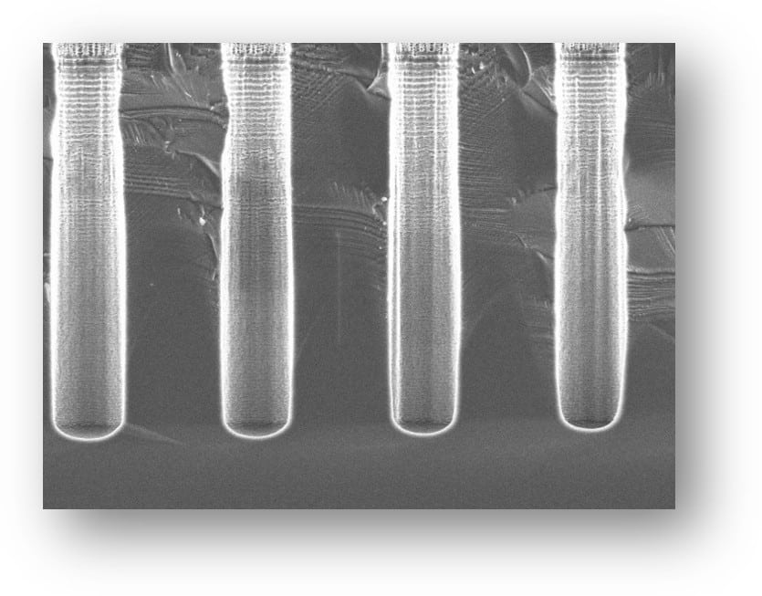
We offer precision etching of dielectrics, metals and semiconductors using Reactive Ion Etching (RIE) and Inductively Coupled Plasma RIE (ICP-RIE) equipment producing high-quality micro- and nanostructures.
We offer wet and dry etching solutions to support a wide range of material etching needs, mainly for silicon. Our advanced dry etching systems use inductively coupled plasma (ICP) and reactive ion etching (RIE) technologies, enabling precise and versatile pattern transfer.
The etching equipment features independently controlled ICP and RF powers, providing flexible control over plasma generation and ion energy, respectively. This flexibility helps to achieve the following:
Thanks to their large plasma area, the tools ensure highly uniform etching across substrates of up to 200 mm in diameter. This makes them ideal for applications requiring high uniformity and reduced substrate damage. These features enable the development of finely tuned etching processes that can be tailored to specific materials and structural requirements.
Examples of etched structures.
TAU has three different etching devices. The main characteristics of each device are introduced below.
UEF has two different etching devices. The main characteristics of each device are introduced below.
"*" indicates required fields
Select recipient for your enquiry: