
We offer advanced optical lithography services, including mask-based lithography for high-resolution patterning, as well as maskless methods such as DLP/LCD-based UV exposure and two-photon absorption direct writing, which are ideal for creating precise 2D and 3D micro- and nanostructures.
Details
Location:
Tampere University (TAU), VTT, University of Eastern Finland (UEF), Joensuu, Oulu, Tampere
Info:
Mask based lithography (TAU, VTT)
In a typical optical lithography process, the substrate is coated with a UV polymer or photoresist, pre-baked, and then loaded into the aligner. The UV light then defines the areas that will become soluble or insoluble to the developer. In top-side lithography, the mask patterns are aligned with existing patterns on the front of the substrate.
In bottom-side lithography, top-side patterns are aligned with existing bottom-side patterns. Before the substrate is loaded, a bottom microscope is used to capture the mask image. After loading, the live bottom-side image is overlaid with the stored mask image to ensure precise alignment. Once aligned, exposure through the mask creates a top-side pattern that matches the bottom side accurately.
Resolution depends on the gap between the photoresist and the mask. Contact modes vary — see the table below. Closer contact improves resolution but increases the risk of contamination. Vacuum contact provides the best resolution, but it can bend the mask and is therefore not usually recommended.
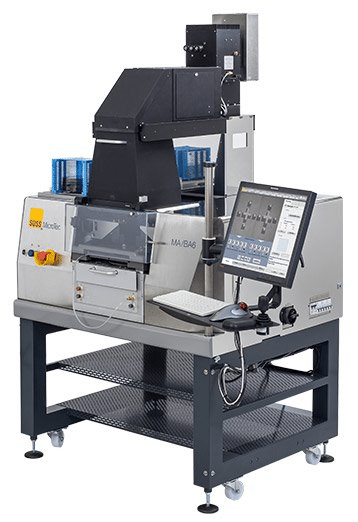
TAU’s and VTT’s Suss MA6 equipment
This equipment can be used for NIL, mask-based optical lithography, and UV-bonding. Please refer to the Nanoimprint Lithography page for more information about the equipment.
Maskless lithography (TAU, UEF)
In maskless lithography, patterns are projected directly onto photoresist using computer-controlled light sources such as digital light processing (DLP) or liquid crystal display (LCD) modulators, or direct laser writing. This process eliminates the need for a physical mask. This process enables rapid design changes and eliminates mask costs, making it ideal for prototyping. In addition to UV-based methods, two-photon absorption using femtosecond lasers as a direct laser writing method enables the fabrication of true 3D micro- and nanostructures with sub-diffraction resolution. Applications include photomask fabrication, maskless wafer lithography, grey-scale patterning, and advanced 3D printing for photonics and biomedical devices. Resolution depends on the optical system and exposure technique used.
Equipment
TAU’s NanoOne 1000 two photon absorption-based lithography equipment
Desktop laser lithography is used to create three-dimensional microscopic features in photoresin materials without the need for photomasks. The lithography system comprises an imaging system, an autofocus system, and a galvo-based system for high-speed scanning. It also features a 2D translation stage for large-area fabrication. This enables structures to be fabricated from various materials with no limitations on the type of substrate.
Specifications:
- Femtosecond fiber laser < 90 fs pulse length, 80 MHz, repetition rate, 250 mW average power, 780 nm center wavelength.
- Long range piezo stage travel range of 120 × 100 mm² and piezo z-stage travel range 49 mm.
- Resolution: minimal horizontal feature size < 200 nm, minimal vertical feature size < 700 nm.
- Writing speed > 500 mm/s.
- Material options: home-made liquid crystal elastomers, UpPhoto, UpBrix, etc.
TAU’s Heidelberg Instruments µPG-501
The device is a DLP-LED based maskless lithography system.
Specifications:
- Exposure wavelength: 375 nm
- Minimum linewidth: ~1.5–2 µm
- Max substrate size: 6″ × 6″
- Max exposure area: 5″ × 5″
- Write speed: 100 mm2/minute
- Substrates: Mask blanks, silicon and glass wafers etc.
- Supported file formats: cif, dxf, gdsii, gerber, bmt, stl
UEF’s Polos µPrinter
The device is µLCD-LED based maskless lithography system.
Specifications:
- Exposure wavelength: 435 nm (alignment at 525 nm)
- Minimum linewidth/features: adjustable from 2 µm up to 23 µm
- Max substrate size: up to 4″ (100 mm) wafers
- Max exposure area: 75 × 75 mm²
- Write speed: prints full substrate in seconds to minutes (speeds vary by resolution)
- Substrates: silicon, glass, metal, plastic, etc.
- Supported file formats: bmp, gdsii, dxf, cif
Send an enquiry
"*" indicates required fields
Select recipient for your enquiry: