Services and tools for the testing of optical waveguide chips and circuits
Details
Location:
Tampere University (TAU), VTT, University of Eastern Finland (UEF), Espoo, Joensuu, Tampere
Info:
Services at TAU in Tampere (Contact person Antti Tukiainen)
Services at VTT in Espoo (Contact person Markku Kapulainen)
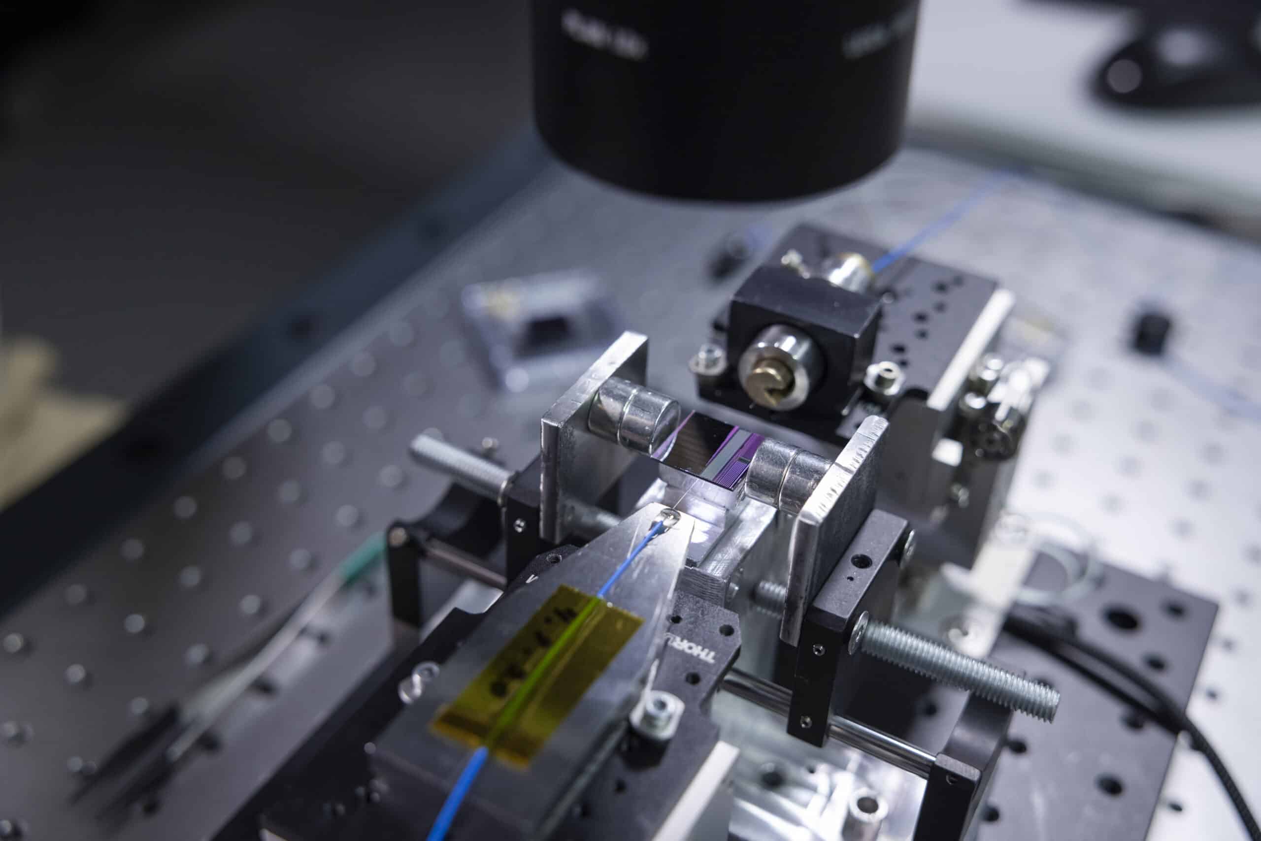
A broad selection of measurement systems are available for the characterization of photonic and optoelectronic components. Systems are available for both chip level (laboratory) and wafer level characterization (laboratory & cleanroom).
We use vibration isolated tables and nanopositioners to reliably couple light to and from devices. The available optical sources and detectors operate over a wide wavelength range. High speed sweeps with tunable lasers or optical spectrum analyzers enable measurement of spectral characteristics.
Electrical sourcing and measurement can be done from low levels (ex. photodiode dark current) to high levels (ex. driving heaters). High speed equipment allows for measurements up to 40 GHz.
Key equipment:
- Anritsu MS9740A
- Santec TSL-550
- Keithley 2450
- Keysight DCA-M N1076A
- Keysight DCA-M N194A
- Wiltron 37369A
- Keysight B1500
- R&S MXO44
- SRS SR865A
Services at TAU in Tampere (Contact person Antti Tukiainen)
- Optical table setups for laser applications and external cavity laser characterisation
- Nonlinear reflectance setup
- Photonic integration and integrated circuits
- High-speed and high-power optoelectronic devices
- Near-to-mid-IR components
Services at UEF in Joensuu (Contact person Pertti Pääkkönen)
Key equipment:
- Anritsu MS9740A (Tunable IR laser 1525 – 1575 nm, https://www.agilent.com/)
- Er-dobed fiber amplifier (EDFA BTO PMF 30 dB, https://www.keopsys.com/)
Send an enquiry
"*" indicates required fields
Select recipient for your enquiry: