
Joensuu

Diffractive Optics
The service includes both scalar and rigorous designing of diffractive optical elements.
Electron Beam Lithography, EBL
We offer the entire fabrication chain or a portion, such as e-beam patterning, according to the customer’s design.
Electron Microscopy
Electron microscopy utilizes an electron beam to study the properties of the sample. Includes scanning electron microscopy (SEM).
Monochromatic light sources
Monochromatic light sources (either continuous wave or pulsed) are commonly employed in the characterization of the functionality of optical elements and in a variety of optical measurements.
Nanoimprint Lithography, NIL
We offer both master element fabrication and nanoimprint lithography services.Optical Microscopy
Transmitted or reflected light microscopy.

Polychromatic light sources
Polychromatic light covers a specific range of wavelengths, and it can be used for spectral measurements.
Raman spectroscopy
Raman Spectroscopy constitutes a non-invasive analytical technique that furnishes intricate insights into chemical constitution, phase transitions, polymorphic variations, crystalline characteristics, and molecular interactions.
Refractive index and thin film thickness characterization
The service includes ellipsometry and prism coupler techniques.
Spectral imaging and analysis
The service includes several techniques for capturing images in such a way that each pixel of the image is recorded as a spectrum.
Spectral imaging of plants
The service includes various spectral imaging methods for plant imaging.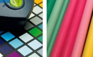
Spectral measurements and analysis
The service includes various spectral measurement and analysis methods.Spectroscopic material characterization
The service includes various techniques to characterize material properties.
Spin coating
Spin coating is a method to apply a uniform film onto a solid surface by using centrifugal force and requires a liquid–vapor interface.
Subwavelength optics
The service includes rigorous designing of metamaterials and plasmonic structures.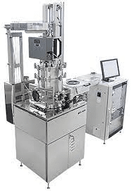
Atomic layer deposition
Picosun Sunale ALD R200 Advanced reactor for deposition of thin films
Characterization of waveguide components
Services and tools for the testing of optical waveguide chips and circuits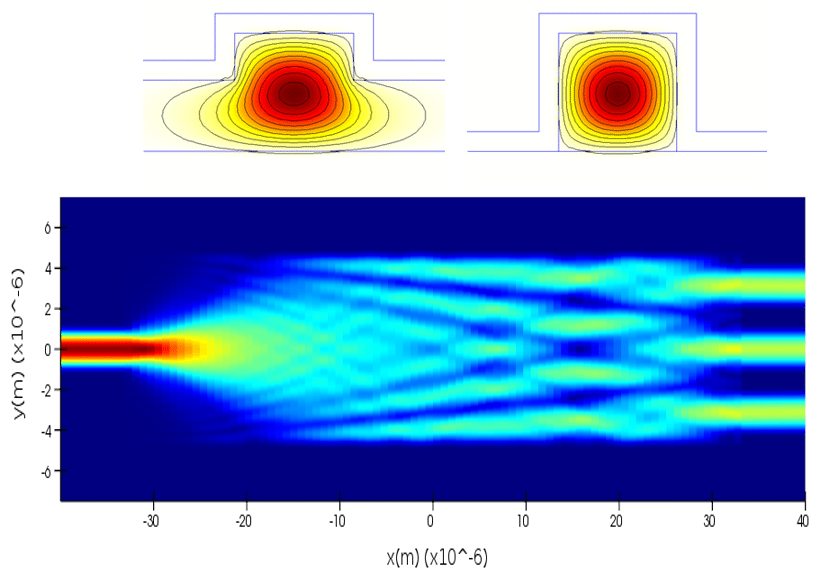
Design of passive waveguide components
Design services for passive waveguide components, such as bends, splitters and wavelength filters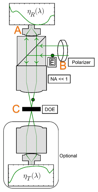
Diffractometry and scatterometry
Charaterization of surfaces based on the diffraction or scattering of light from the surface.
Lens and optical systems design
The service covers the design of lenses and optical systems.
Mechanical surface profilometry
Measuring sample surfaces with a contact probe is fast and accurate method for most surfaces.
Nextron Micro Probe test chamber
Test chamber enables electric measurements of a sample under controlled environment and illumination.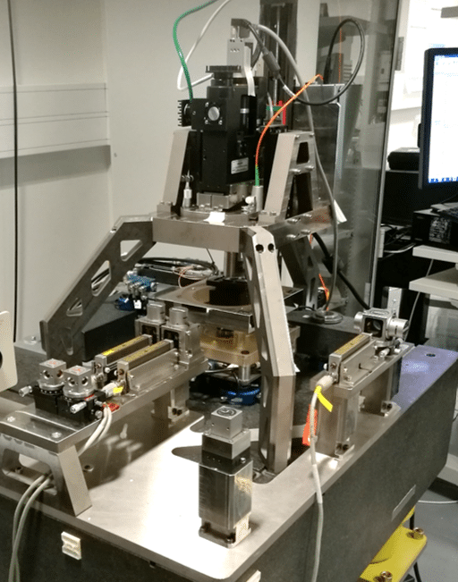
Optical surface profilometry
Optical profilometers enable contactless measurement of surfaces.
